This post is part of the “Learning Flash: For Storage Engineers” series. Click here, if you missed the intro post.
Finally, my friends, we are getting to the good stuff. In this post, I’ll be discussing how the greatest limitation of the transistor (data-loss after power-loss) was overcome by introducing some additional components into the transistor. I remind you that modern day flash cells are 10’s of nanometers in size and the mechanics by which they store and retrieve data occur at the sub-atomic level. Very, very impressive when compared to how mechanical storage works. Lets jump right in!
The first thing you should be aware of is that there are a few more components added to the transistor to enable non-volatility in NAND. The cell structure of (Single-Level-Cell) SLC and (Multi-Level-Cell) MLC is identical, but I’ll only be describing SLC behavior below to keep things simple at first. I’ll go into MLC behavior in a later post.
- Floating Gate: Stores electrons while the cell is programmed. Stored electrons then generate a counter electric field that partially screens the electric field produced by the control gate.
- Tunnel Oxide: This is a weaker insulator that, given a strong enough voltage differential, can allow electrons to “tunnel” through. Acts as a valve, only allowing electrons to pass into and out of the floating gate when desired.
- Blocking Oxide: This isn’t necessarily new–it is a similar insulator like what was used in the transistor. It is a strong insulator that prevents electrons from passing all the way through the floating gate and continuing on into the control gate.
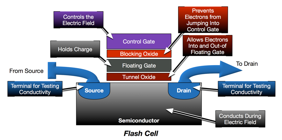
*Many current-generation flash cells actually have evolved into what is known as a Charge-Trap Flash design. Charge-Trap Flash replaces both the floating gate and the tunnel oxide with a single high-k dilectric layer that is acts as both the weak insulator and the floating gate. This approach allows greater density and reliability in flash cell designs. Further advancements currently underway include moving flash from a planar architecture into a 3 dimensional design. I will go into more detail on this later.
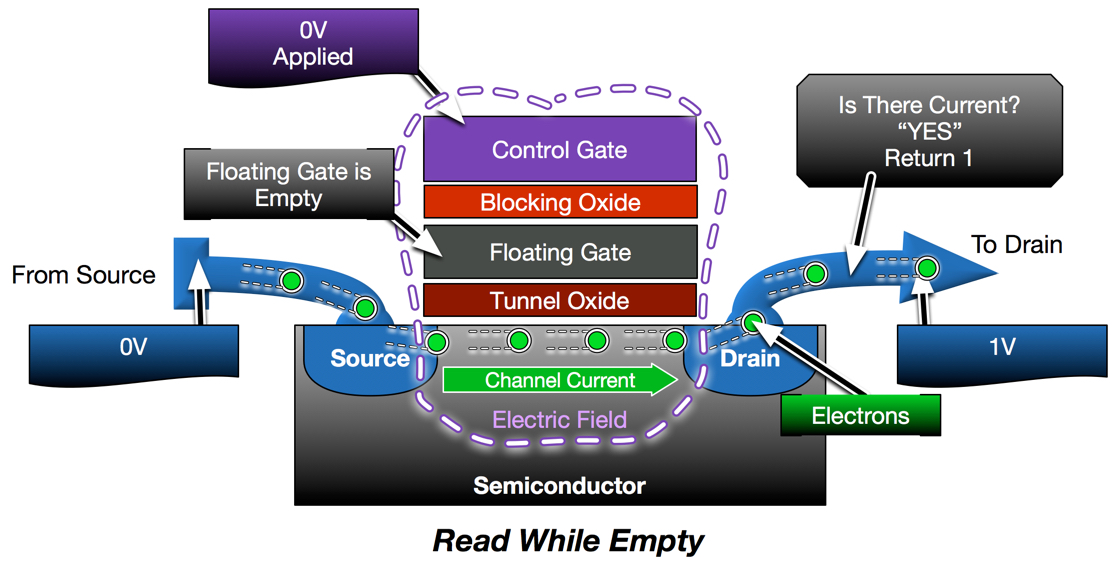
The first operation I want to show you is actually an un-programmed (empty) cell. I’m starting with an empty cell, because it functions just like the transistor on the prior post. The floating gate’s job is to provide interference between the control gate and the semiconductor when charged. In an un-charged cell, there is no interference so control gate voltage causes the semiconductor to conduct just like a basic transistor. This would represent a 1 in binary.
So how do we get electrons into the floating gate? For NAND, this is done through a method known as Fowler Nordheim Tunneling. It is complicated, but as a storage engineer, you don’t need to know how all sausage gets made. Therefore, here is simple explanation.
During a program operation, a high voltage is applied to the control gate. This creates a high voltage differential and strong electric field. The voltage is sufficiently high to pull electrons from the semiconductor substrate, through the tunnel oxide (weak insulator), and into the floating gate. The blocking oxide located between the floating gate and the control gate to prevent those electrons from passing straight through the floating gate and draining out the control gate.
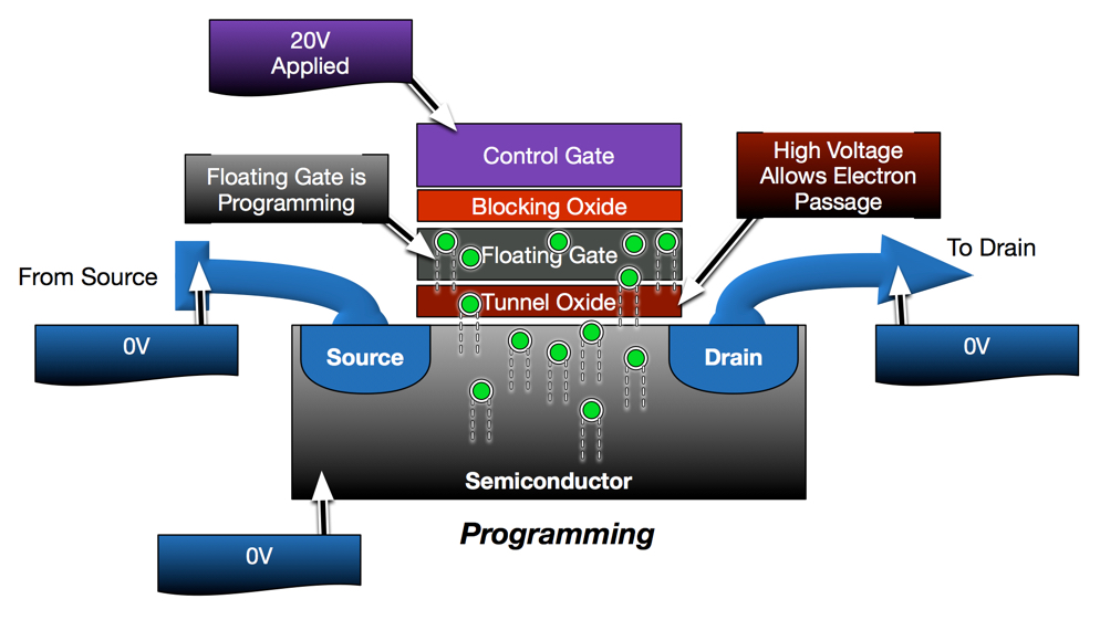
When the program operation completes, and the voltage on the control gate is dropped, the electrons don’t have enough energy to pass back through the tunnel oxide. They are trapped in the floating gate until a future erase operation. Most importantly, while they are trapped within the floating gate, the generate their own electric field. This field will later interfere with future conductivity tests to indicate the cell is programmed.
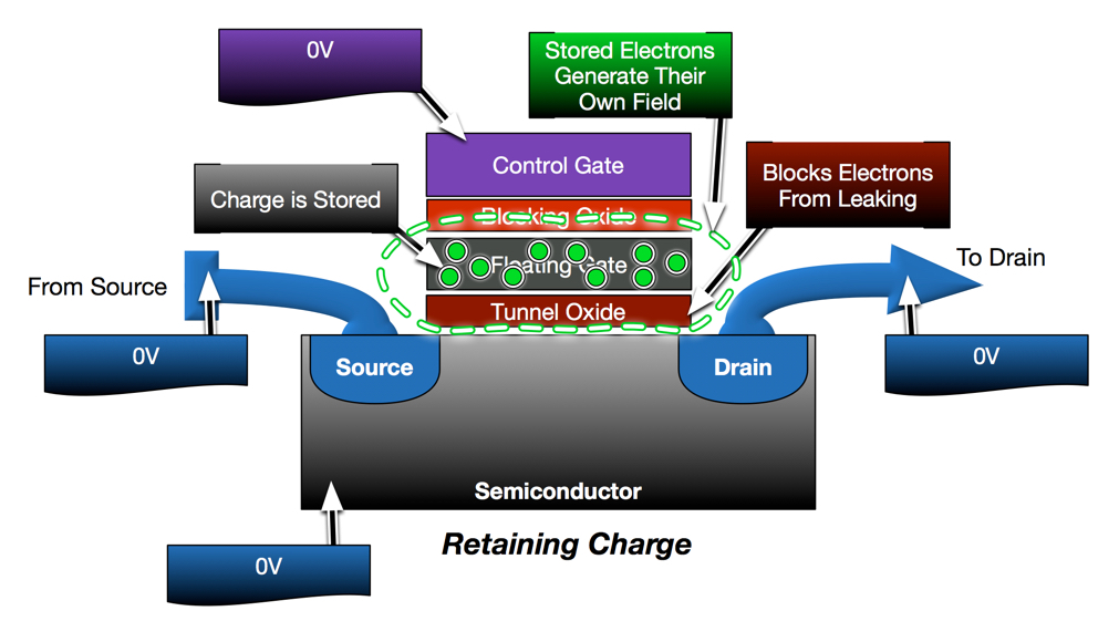
When programmed, the cell responds differently to read requests. Like before, a voltage differential is applied between the source and drain and a small voltage is applied on the control gate. If the cell were empty, the electric field generated by the control gate would be enough to cause the semiconductor to conduct. However, the presence of electrons in the floating gate creates a counter-field (or screen), which partially blocks the electric field from the control gate. The screened electric field is no longer sufficient to establish conductivity and the cell returns 0, indicating it is programmed.
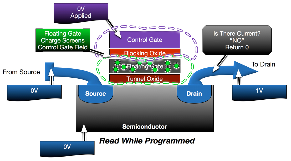
Do keep in mind that the floating gate screen is not absolute. In transistors and NAND there is a concept of a voltage threshold, which is the control gate voltage required to cause conductivity. By charging the floating gate, we increase the voltage threshold so the cell won’t conduct when a low voltage is applied. But even with a programmed cell, we could increase the control gate voltage to a point where it would over-power the effects of the floating gate and cause the channel to conduct regardless.
MLC: The amount of charge in a cell will also affect the threshold voltage required to allow conductivity. Multi-Level-Cell (MLC) Flash, which allows 2 bits per cell instead of 1 bit, use this principle. MLC cells can contain different levels of charge within the floating gate. The amount of charge can be tested by stepping up the control voltage until conductivity occurs. This threshold voltage is then decoded into a binary result. More on this later…
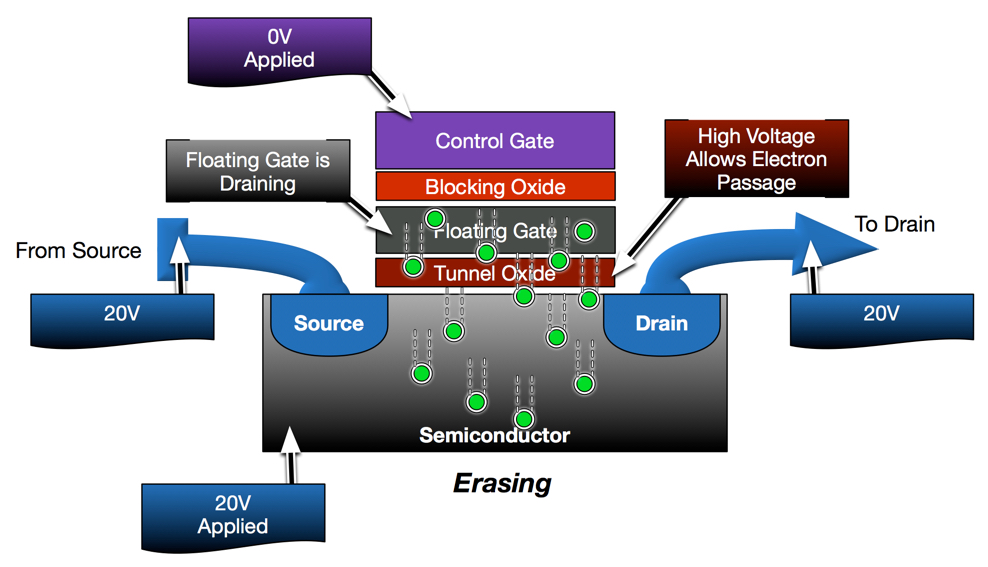
Finally, the cell can be erased by reversing the processed used to program it. The control gate voltage is held at ground while a strong voltage is applied to the semiconductor substrate (also known as bulk terminal). The voltage is sufficiently high enough to cause the electrons to jump back through the tunnel oxide and drain through the substrate leaving the floating gate empty.
This post describes the basics of how flash cells are programmed, read and erased. However, these functions are not as simple as they appear. The story of NAND is one of 3 conflicting goals; density, cost and reliability. In order to provide the low cost, highly dense and highly reliable NAND we put in our datacenters today there are a lot of problems that need to be worked out.
In the next post, I’ll discuss the many challenges of flash storage and how working through those challenges exposes new ones. Thanks for reading! Comments and questions are always welcome.
 Dale Carnegie: How To Win Friends and Influence People
 Dave Ramsey: The Total Money Makeover: A Proven Plan for Financial Fitness