This post is part of the “Learning Flash: For Storage Engineers” series. Click here, if you missed the intro post.
I apologize for the entirely inexcusable delay between posts in this series. I had every intention of getting this post completed earlier this year, but life and work have both been very busy. Better late than never, I suppose…
In the previous post, I demonstrated how the transistor has been modified to enable non-volatile data retention. I also showed how flash cells are programed, read and erased. At first glance, flash seems pretty simple and, if density and cost were of no consequence, flash would have remained this simple.
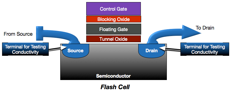
If we take another look at the basic model of the flash cell, you will notice it has 2 dedicated terminals. This sort of architecture, where each flash cell–each bit–is individually programable is referred to as NOR. The granularity of addressability makes programming NOR much easier. The dedicated terminals that provide per-cell addressability, however, also greatly increase the space, circuitry and costs required for NOR.
While NOR flash is very flexible, the required size and materials make it cost-prohibitive as a disk alternative. To replace disk, we needed to make some compromises to get cost and density down to comparable levels. This is where NAND comes in.
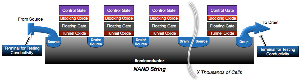
The first compromise we find in NAND architectures is the loss of per-cell programming granularity. Instead of flash cells each having their own dedicated source and drain terminals, the are instead connected in a serial string. This is a similar concept to a string of christmas lights, where every light in the string participates in the circuit. For a light in the middle of the string to receive current, all other lights in the string must also receive and pass current. If any light does not pass current, the entire string fails. Likewise, NAND flash is formed in long strings of transistors. Programming and reading any one cell requires the entire string to participate.
NAND is designed this way because it greatly reduces the circuitry required for flash. Instead of placing terminals for each cell, the terminals can be placed at the ends of strings containing 32 or 64 of cells. This results in much greater density within the flash die and significantly reduced costs. Further density is achieved by sharing control gates across rows of strings to form a block. I’ll go into more detail on the NAND block later in this post.
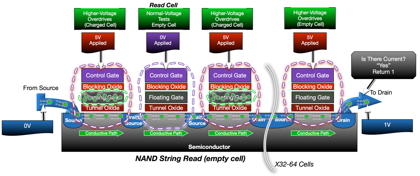
As described in my prior posts, a read operation is a basic conductivity test. If a flash cell is programmed, the charge in the floating gate will inhibit conductivity, resulting in a “programmed” response. Empty cells will not interfere, resulting in conductivity. The challenge with NAND is that a read operation on any one cell in the string requires the rest of the string to be conducting. This is accomplished by placing higher, overdrive voltages on the control gates of other cells in the string in order to force conductivity regardless of their programmed state.
Voltage Thresholds are the key to flash operations. A voltage threshold is the difference in voltage required to allow for the movement of electrons. An empty cell has a lower voltage threshold (slightly negative, actually) than a programmed cell because the charged floating gate interference increases the voltage differential in a programmed cell. Therefore, a cell can be tested(read) by using a control gate voltage that is slightly higher than that of an empty cell, but lower than a programmed cell. Using this same principle, even a programmed cell can be forced to conduct, regardless of programmed state, by using a high enough voltage.
In the below diagram, the second cell in the string needs to be read. In order to test this cell, the rest of the string must be forced into conductivity. While 0V is applied to the control gate of the cell being read, 5V is applied to all other cells to force conductivity regardless of whether they are programmed. Since the cell being read is not programmed, it conducts and results in a current through the string which is sensed and interpreted as a “1”.
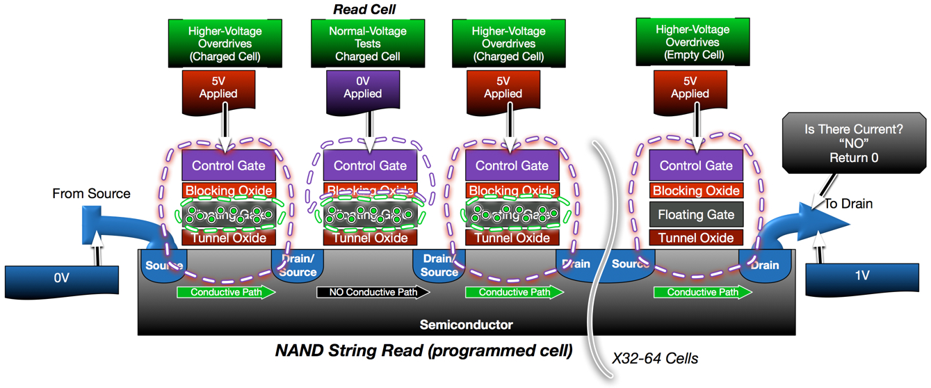
If the same read operation is performed on a cell that has been programmed a different result is measured. All non-read cells are still forced to conduct with 5v. The charged floating gate on the read cell is enough to inhibit the low voltage being applied to that control gate. As a result, the read cell does not conduct. Without a complete conductive circuit, the string does not pass current which is sensed and interpreted as a “0”.
The NAND Block: Let’s get complicated!
Up until this point, I have been modeling flash architectures from the perspective of a single string. While it is easier to learn about the fundamentals using a basic string model, now we must zoom out a bit to look at how NAND operates within the larger structure of a NAND block.
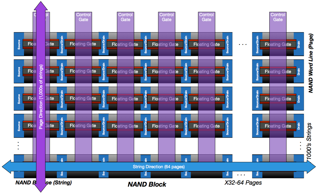
A block , also known as an erase block, is a collection of flash cells organized into a planar grid. In one direction, the string direction, cells are aligned to the semiconductor between source and drain terminals located on opposite ends of each string. This is also referred to as the bit line. Intersecting with the cells along the bit line are the shared control gates which form the second set of lines used in page referencing. Pages are also referred to as word lines. By sharing source and drain terminals in the string direction and sharing control gates in the word direction, the circuitry within a NAND block can be kept to a minimum.
Strings (bit lines) typically only contain 64 cells, whereas control gates can connect across thousands of cells based on the page size of the NAND (4k, 8k,16k, etc..). Consequently, program and read operations occur at the page granularity.
Page Sizes typically increase over time as flash die’s become more dense. A 64GB drive may use a page size of 4K, whereas a 512GB drive may use a page size of 8K. Contrast this to HDD sector granularity, which has long been 512bytes. This continual shift in page size as new drives are released creates foundational architecture problems for storage array manufacturers that didn’t exist with HDDs. I’ll discuss these in more detail in a later post.
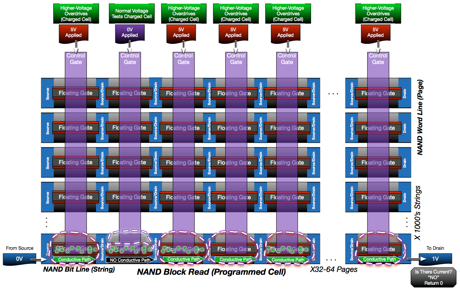
In order to help orient you to the grid diagram vs the string diagram, below is the same read operation on a programmed cell that was diagramed previously in the string view.
The tight orientation of NAND makes it more susceptible to disturbances during read and program operations. This is a fundamental challenge of NAND; the more tightly we pack the components for density, the greater the challenge in ensuring reliability.
In the above diagram, notice how the control gate voltages are applied across all strings, not just the selected string being read/tested. Since all strings share the same control gates, this can’t be avoided. Over time, the voltage increases shared with non-selected strings causes electrons to slowly attach to other non-programmed cells in those strings. After 100’s of thousands of reads, weak charge build-up can cause un-programmed cells to hold some charge and begin to interfere with read accuracy. To ensure this read disturbance never becomes a problem, reads per page must be counted and monitored. Any blocks with page reads over safe limits should have their contents written to a new block so the old block can be erased. Read disturbance is not permanent. Erasing a block resets the cells with read disturbance charge build-up and restarts the read counter to zero.
Cell programming is also significantly more complex within a NAND block. High voltages are required for NAND cell programming, which create high voltage differences throughout the tightly organized NAND block. Even more so than read disturbance, high voltage differences during programming can cause electrons to accumulate on un-programmed, un-selected cells which later appear as a weak charge. Just like read disturbance, program disturbance must be carefully accounted for during program operations.
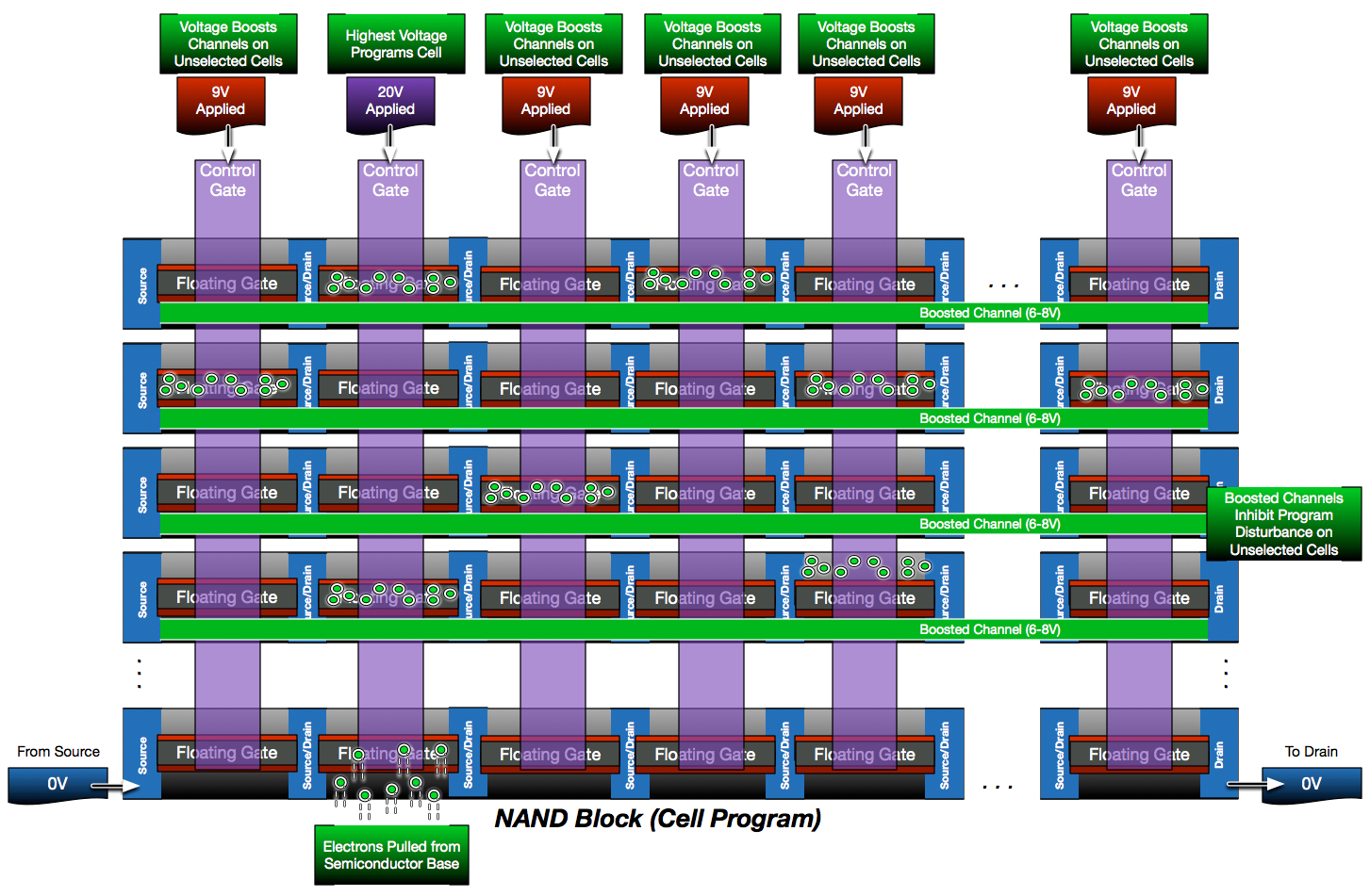
To reduce disturbance, the voltage differences within the NAND block have to be partially balanced during program operations. Today this is most often done with a concept called self-boosted inhibit. Self-boosting involves applying a moderate voltage to the unselected control gates throughout the NAND block while also electrically isolating the unselected bit lines. This creates a capacitive coupling that raises the channel voltage of the unselected strings and reduces the likelihood for program disturbance in those cells.
Any remaining read or program disturbances are identified and compensated for through ECC (Error Correcting Code).
Erase operations on a NAND block are relatively simple. The semiconductor base (also known as the well) that supports the channel for each cell is actually shared across all cells. As indicated before, the semiconductor base is where electrons migrate from during programming. It is also where electrons migrate to during erase operations. To erase the block, all control gates for the selected block are held at 0V while a strong positive voltage is applied to the entire well. This creates a voltage differential that pulls the electrons from the floating gates and pushes them back into the well.
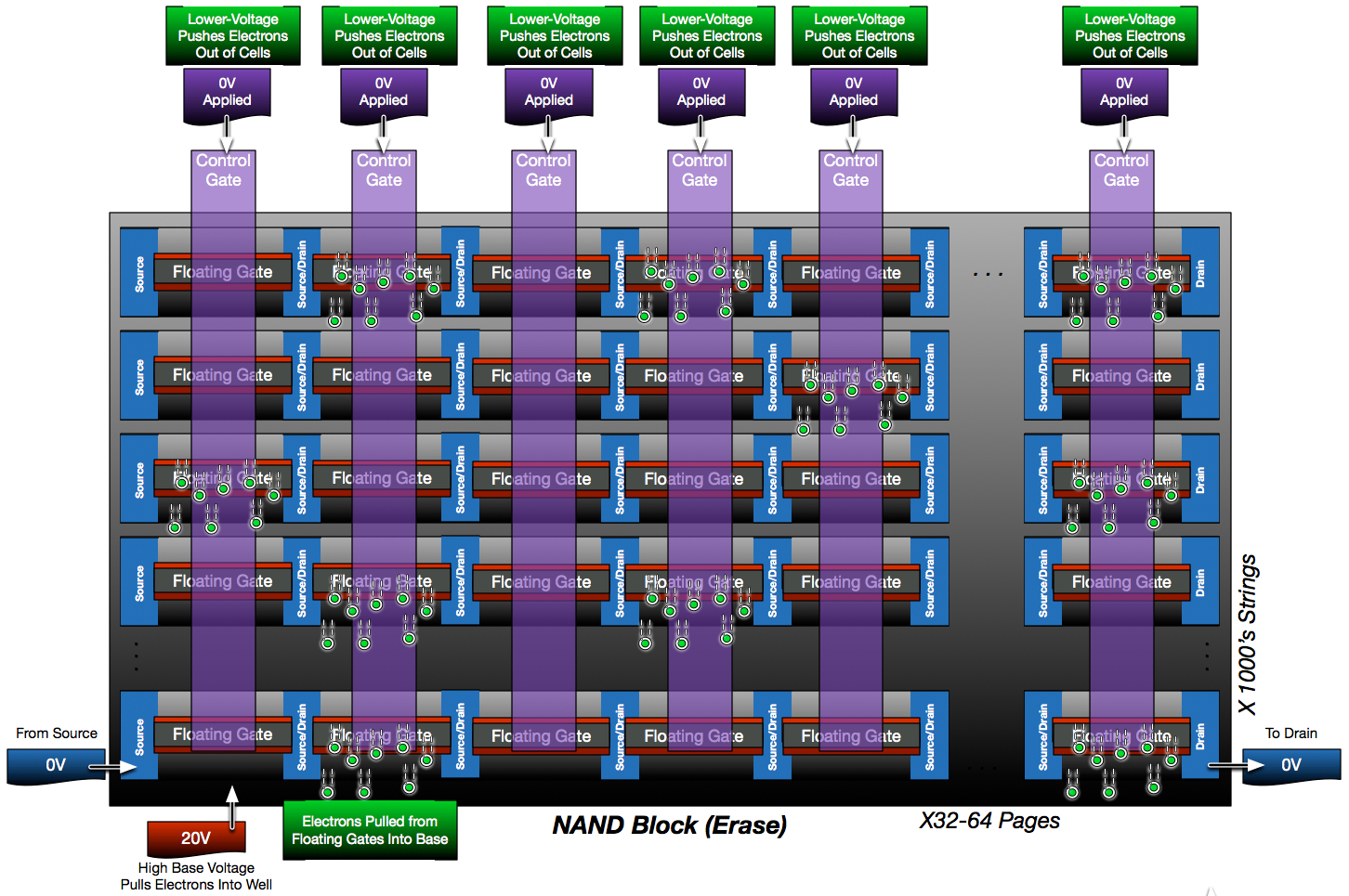
Erases are made simple because they target the entire block, not individual cells or pages. This simplicity comes at a cost, however. Unlike disk, the contents of a flash cell cannot be modified without first erasing that cell. Since erases are only performed at a NAND block granularity (8+MB in size), this creates more challenges that storage controllers must compensate for when overwriting flash media. I’ll discuss this more in a later post.
Moar Density!
Density improvements haven’t stopped at NAND alone. The vast majority of flashed used in storage arrays today is Multi-Level Cell Flash. The physical structure is nearly identical to traditional Single-Level-Cell Flash, but MLC media stores more than one bit per cell by varying the actual amount of charge within the cell. Whereas SLC has 2 bit positions (charged and not-charged), MLC has 4 bit positions (charged, mostly-charged, mostly not-charged and not-charged). MLC provides double the density but requires much more sophisticated programming logic and is far more sensitive to electrical variations than SLC.
MLC programming requires the cell to be programed and tested in multiple, incremental steps before achieving the desired charge level. Read operations require multiple passes on the cell as well in order to accurately determine the cell’s charge. This is why MLC media is slower than SLC for program and read operations. It is also why it wears significantly faster than SLC.
Triple-Level Cell Flash is provides triple the density over SLC with 8 bit positions (voltage levels). TLC requires even more interaction with the flash cells during programs and reads which makes TLC the slowest of the NAND media. It also wears significantly faster than MLC making it suitable primarily for workloads with minimal overwrites such as archive.
The most significant breakthrough in recent NAND technology is 3 dimensional (or vertical) NAND. Whereas NAND has historically been organized in a 2 dimensional, planar design; 3 dimensional NAND stacks flash cells vertically as well as horizontally. It is the equivalent of replacing motels with skyscrapers. This new dimension in NAND scaling allows for individual flash cells to actually become larger while still increasing the density of the NAND overall. Larger cells mean components are less tightly packed which translates directly to greater reliability. The 3-dimensional design also gives control-gates greater surface area with the floating gates which makes the flow of electrons into and out of the cells even faster. The result is a denser, faster and more reliable NAND. This technology is just now starting to appear in enterprise arrays and I’m excited to see how it further transforms the storage industry.
Creating a high performance, high density, reliable and low-cost storage medium requires a lot of intuitive engineering and is not without some compromises. I hope this series helps underscore the amount of engineering effort involved in bringing this revolutionary technology to market at a price and size where everyone can benefit.
Comments and questions are always welcome!
 Dale Carnegie: How To Win Friends and Influence People
 Dave Ramsey: The Total Money Makeover: A Proven Plan for Financial Fitness